
Energy harvesting through thermoelectrics: topological designs and materials jetting technology


Abstract
The vast amount of waste heat released into the environment, from body heat to factories and boilers, can be exploited for electricity generation. Thermoelectrics is a sustainable clean energy solution that converts a heat flux directly into electrical power and vice versa and therefore has the potential for both energy harvesting and cooling technologies. However, the usage of thermoelectrics for large-scale applications is restrained by its device topologies and energy conversion cost efficiency trade-offs. The increase in complex topological designs reported in literature shows a shift towards customizability and improvement of thermoelectric devices for maximum energy conversion efficiency. Increasing design complexity will require an innovative, cost-effective fabrication method with design freedom capabilities. In light of this, this review paper seeks to summarize various thermoelectric topological designs as well as how 3D Printing technology can be a solution to the fabrication of cost- and performance-efficient thermoelectric devices. Specifically, as a process category of 3D Printing technology, Materials Jetting will be elaborated for its usefulness in the fabrication of thermoelectric devices. With in-depth research in materials jetting of thermoelectrics, the gap between small-scale materials research and scaled-up industry applications for energy harvesting through thermoelectric devices is expected to be bridged.
Keywords
INTRODUCTION
The escalating demand for electricity, coupled with limited reserves of fossil fuels, calls for a vital transformation toward renewable energy production. There is a pressing need for sustainable solutions to cater to our increasing electricity demands. At the same time, in factories and manufacturing processes, up to 50% of the energy consumed is released into the environment as waste heat through hot exhaust gases and liquids[1]. In the United States, 5-13 quadrillion Btu (1015 Btu)/year of waste heat energy is emitted and unrecovered[1]. These copious amounts of untapped waste heat can be exploited for conversion into useful work in factories or the conversion into electrical supply. Waste-heat recovery technologies such as the Rankine cycle[2] and heat pump systems[3] often require the intermediate step of converting waste heat into mechanical energy for pumps and fans before producing useful work. On the other hand, thermoelectrics (TE) offers itself as a class of materials that inter-converts heat and electricity and thus has the ability for energy harvesting/cooling solutions. In the presence of a temperature gradient, TE materials generate an electrical potential difference, providing direct electrical energy from heat sources. The absence of moving parts allows for easy maintenance and excellent reliability while providing sustainable electrical energy to power devices. Besides harvesting waste heat from factories, heat from photovoltaic cells[4] and high-power light-emitting diodes[5] have also shown potential for energy conversion through TE devices. On a smaller scale, a small temperature difference between the human body heat (waste heat energy) and the environment is also able to generate usable energy to power wearable electronic devices[6-12].
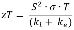
where S is the Seebeck coefficient, σ is the electrical conductivity, T is the absolute temperature, and kl and ke represent the lattice and electronic thermal conductivity, respectively. A high-performance TE material should have a high power factor (P.F = S2·σ) and a low total thermal conductivity (k = kl + ke). However, due to the mutual interdependency of these two properties, the optimization of zT is extremely difficult. Over the past decades, the enhancement of zT has been done primarily via engineering electronic or thermal properties. In terms of electronic properties, strategies such as band engineering and resonant doping are popular in improving the power factor[13-15]. Improvement of thermal properties can be achieved through the suppression of kl using point defect scattering, nano-structuring, and lattice anharmonicity[16-21]. Low thermal conductivity often originates from the result of weak chemical bonding, which in turn affects the mechanical strength of the TE material. Specifically, for a thermoelectric generator (TEG), the efficiency of the heat-to-power conversion (η) is expressed as:
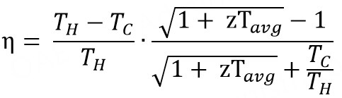
On each end of a TEG device, it will be subjected to a hot and cold side. The zTavg is the average figure of merit between the hot side temperature (TH) and the cold side temperature (TC).
Optimizing zT involves judicious materials selection and, importantly, well-designed fabrication processes[22,23]. The overall device architecture/topology is also an important aspect of efficient structural behavior and application-focused usage. Current fabrication methods of fabricating TE legs are via spark plasma sintering and hot pressing[24-27]. These methods produce bulk TE ingots, thus restricting the geometrical complexity and the eventual energy harvesting/cooling application areas. TE device topologies need to be customizable and varied in order to increase the utilization of thermoelectric devices for different applications. As such, to increase the complexity of TE device topologies and its fabrication freedom, 3D printing is an attractive alternative fabrication method. Therefore, in this review, the applications of thermoelectrics with different topological designs will be discussed, along with their advantages and limitations. Specifically, planar TE designs will be highlighted for their usefulness for wearable self-powered electronics. To ease the processing costs and increase the material efficiency, 3D printing technology will be introduced as an emerging technique for cost-effective fabrication of thermoelectrics. Due to the rising trend of electronics 3D printing through Materials Jetting (MJ) technology, emphasis will be placed on the materials selection for materials jetted TE and the ink properties for a successful printing. Lastly, the outlook in the field of materials jetted TE for energy harvesting applications will be discussed.
TOPOLOGICAL DESIGNS FOR THERMOELECTRICS
There are two main topologies for TE devices, namely the vertical (or sometimes referred to as “π”) and planar (or “lateral”) arrangement of the thermopile, as illustrated in Figure 1. In both arrangements, the legs (also known as thermocouples) are made of alternating p-type and n-type thermoelectric materials and connected electrically in series and thermally in parallel.
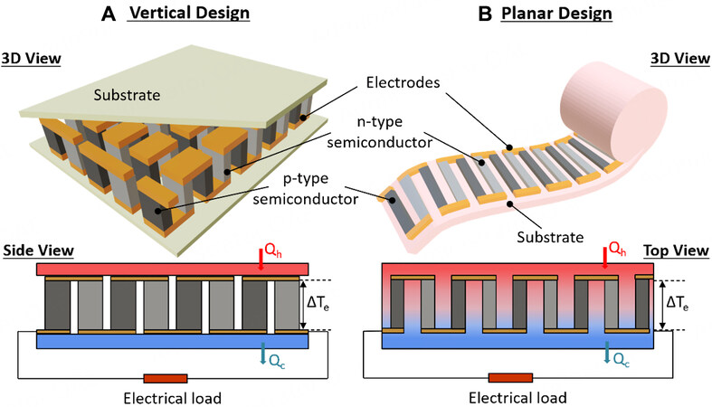
Figure 1. Topological designs and schematic diagrams of heat flow for (A) vertical design, and (B) planar design of thermoelectric devices.
In a vertical TEG design, thermocouples are arranged vertically along the heat flow direction Qh-Qc [Figure 1A]. The effective temperature gradient which gives rise to the Seebeck effect of the TEG is expressed as ∆Te (i.e., the difference in temperature of the hot and cold side). Vertical TEGs have high thermocouple integration and generate a high output power[28]. In comparison, vertical thermoelectric coolers (TECs) operate according to the Peltier effect, whereby a passing current creates a temperature difference across the thermoelectric device. Thus, TECs are most commonly used as Peltier modules for refrigeration in chillers, DC machines and power plants[29]. Conventional vertical TEGs and TECs are assembled via wire cutting and soldering of the metal interconnects between each thermocouple.
On the other hand, thermocouples in a planar TEG/TEC are deposited on substrates in the direction of lateral heat flow Qh-Qc [Figure 1B]. Compared to the vertical arrangement, a planar arrangement benefits from its fabrication adaptability and versatility on many substrates (IC chips, flexible substrates, curvatures, and textiles). Therefore, planar design finds its usefulness as micro-coolers and microgenerators in the electronics industry and wearables applications. This design is especially useful for waste body heat harvesting to self-power electronics. Conventionally, planar TE devices are fabricated via screen printing[30,31], electrochemical deposition[32,33] and physical vapor deposition such as co-evaporation[34,35] and magnetron sputtering[36,37].
It should also be noted that, in addition to the conventional TE designs, unique device architectures have been developed in recent years, which could lead to material-efficient devices with maximized power output. For example, O’Connor and colleagues demonstrated a new thin-film thermoelectric architecture that combines the merits of both a vertical and planar TE device, as shown in Figure 2A[38]. The corrugated design allows a substantial temperature difference across the thermoelectric leg. Finite element computational models of trapezoidal wave structures were developed to study the effect of geometric parameters of the corrugated TE design on thermoelectric cooling performance. The study shows that with design geometry optimization, the corrugated device has comparable performance to conventional thermoelectric materials and has high potential for flexible device applications. In another work, Lemmer and colleagues introduced the concept of origami TEGs whereby the folding of the substrates provide electrical insulation between TE elements without the need for a flexible polymer matrix as the insulating material, thus reducing the device’s parasitic thermal conductance [Figure 2B][39]. By altering the print layout, maximum power output can be achieved via thermal impedance matching of the TEG to the heat source and heat sink. In addition, Y-type TE structures were proposed by Ono and colleagues
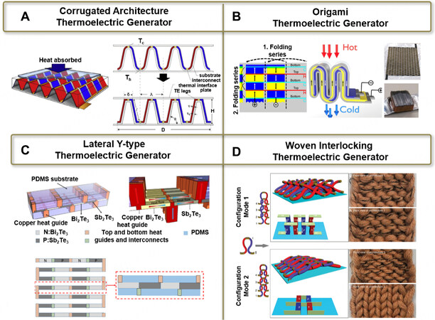
Figure 2. Nonconventional thermoelectric device topologies reported in recent years. (A) Corrugated TEG, adapted with permission from[38], (B) Origami TEG, adapted with permission from[39], (C) Y-type TEG, adapted with permission from[40] and (D) woven interlocking TEG, adapted with permission from[41].
ADDITIVE MANUFACTURING FOR FABRICATION OF COMPLEX THERMOELECTRIC STRUCTURES
To increase the industrial implementation of energy harvesting through TE devices, its processing costs and energy conversion performance must be competitive. Compared to labor-intensive conventional fabrication routes, Additive Manufacturing (AM) is a fitting manufacturing technology for the advancement of cost-effective high-performance TE devices. Coupled with minimal material wastage, high-throughput process and geometrical flexibility, it is timely and appropriate for extensive research into additively manufactured thermoelectrics. To expedite this research area, it is important to understand the different AM technologies, with their merits and weakness, as a methodological approach in effectuating additive manufactured thermoelectrics for industrial applications.
As shown in Figure 3, AM technology can be broadly classified into 7 main process categories - Binder Jetting, Directed Energy Deposition (DED), Material Extrusion, Material Jetting (MJ), Powder Bed Fusion (PBF), Sheet Lamination and Vat Photopolymerization (VP). Each process has found its influence in several major applications. For instance, in dentistry, VP has seen exponential interest and utilization. The significant reduction in manufacturing time for bridges and crowns, coupled with its excellent surface finishing and resolution, has led to the adoption of VP in many dental clinics and laboratories[42,43]. DED and PBF techniques have already been used extensively to manufacture customized metal parts in the repair of aerospace components[44]. However, as compared to Materials Extrusion and MJ technology, DED and PBF have higher equipment costs due to their system requirements. In relation to thermoelectrics, there is no singular AM method that can optimally print both vertical and planar TE designs. Depending on the topology of TEG for its required application, different 3D printing techniques are listed in Table 1.
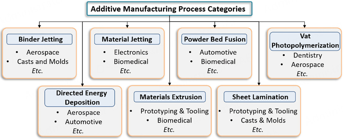
Figure 3. The 7 main Additive Manufacturing process categories. Each process category has its strengths for different industrial applications.
Comparison of the 7 Additive Manufacturing process categories for the two main topologies of TE devices
| Topology | 3D printing method | State of TE material feedstock | Surface finishing of printed structures | Post-printing TEG assembly required | Advantages | Disadvantages |
| Vertical arrangement | Materials extrusion | Liquid-based/Filament-based | Poor | No | 1. Ability to generate high electrical power | 1. Limited device flexibility 2. Difficulty in reducing size due to assembly problems 3. High manufacturing costs of powder-based 3D printing methods |
| Powder bed fusion | Powder-based | Good | Yes | |||
| Directed energy deposition | Powder-based | Good | Yes | |||
| Vat photopoly-merisation | Photocurable liquid-based | Good | Yes | |||
| Binder jetting | Powder-based | Poor | Yes | |||
| Planar arrangement | Material jetting | Liquid-based | Excellent | No | 1. Deposition on many substrate materials (including flexible substrates) 2. Cheaper manufacturing process | 1. Difficulty in generating high temperature difference 2. Low electrical power generated |
| Sheet lamination | Liquid-based | Excellent | No |
Several 3D printing methods have the ability to fabricate highly hierarchical and material efficient thermocouples for vertical TE devices, as shown in Table 1. However, most of these 3D printing methods (such as PBF, DED, VP and Binder Jetting) still require post 3D printing assembly of the integrated TE device. Currently, Materials Extrusion technique is the most reported 3D printing method to print TE materials such as bismuth telluride (Bi2Te3)-based materials[45,46] and compositionally segmented TE legs[47]. Materials Extrusion technique also has the potential to fabricate an entire vertical TE device through alternating nozzle printing. However, the thermal expansion mismatch between the different materials during the heat treatment process still poses a technical challenge in multi-material 3D printing research area. Furthermore, the “stair-step” effects of Materials Extrusion technique and surface roughness of binder-jetted printed parts greatly damage the resultant structural quality of 3D thermoelectrics structures.
On the other hand, techniques such as MJ and Sheet Lamination are unable to build thermocouples with a high aspect ratio. However, these techniques allow printed TEs to have high levels of printing resolution and excellent surface finishing. These techniques also show potential for the printing of integrated planar devices as they are relatively mature technologies for multi-materials fabrication. The lack of need for post-printing assembly solves a major problem in thermocouples and electrode adhesion and contact resistance required in TE assemblies. These traits thus make planar TE devices for self-powered/cooling electronics and wearable applications viable through these 3D printing fabrication methods.
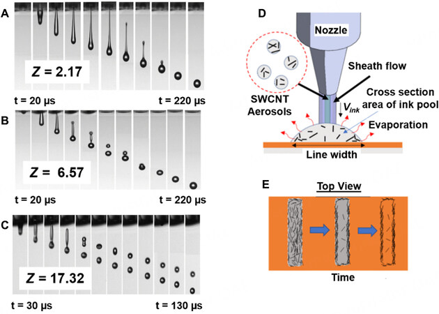
More specifically, MJ has been gaining momentum as an alternative candidate in the field of electronics 3D printing due to its precise deposition and high resolution of printed features. According to ISO/ASTM 52900, MJ is defined as an additive manufacturing process in which droplets of feedstock material are selectively deposited. Within MJ, there are a few distinct techniques such as Drop-on-Demand (DoD) Inkjet Printing, Nanoparticle Jetting (NPJ), Polyjet[48] and Aerosol Jetting[49]. While Polyjet is mainly used for polymeric prototyping and tooling, DoD inkjet printing, NPJ and Aerosol Jetting have main applications in electronics material jetting. A tremendous amount of research effort has been poured into the development of flexible and stretchable nanoelectronics and bioelectronics through Materials Jetting, in particular, DoD Inkjet Printing and NPJ. DoD Inkjet Printing is an established printing technique that deposits ink via a thermal or piezoelectric system[50,51]. NPJ, on the other hand, jets inks containing metal or ceramic nanoparticles on a heated build platform, allowing the solidification of nanoparticles for better handling and post-printing treatments. Solidification of material jetted structures can range from ultra-violet light assisted, infrared light and thermal assisted[52]. In addition, there is ongoing research into reactive jetting technique to increase the printed part strength[53]. In contrast, Aerosol Jetting is a relatively newer MJ technique that has been gaining recognition as a fabrication technique for electronics printing. This droplet-based method deposits an aerodynamically focused aerosol jet stream carried from an aerosol mist reservoir[54]. This technique allows feature size of less than 10 µm with thickness from 100 nm to several millimeters, making it suitable for printing interconnects, antennas, and sensors[49]. In addition, the versatility of 5-axis systems (e.g., Optomec Aerosol Jet) has great potential for electronics printing on complex substrates and surfaces. Despite the differences in the droplet formation and solidification methods, these techniques serve to build structures from material droplets, forming the broad MJ technique process category.
Materials selection for materials-jetted thermoelectrics
The selection of material plays an important part in the fabrication of high-performance and flexible thermoelectric devices. For inorganic materials, 1D nanostructured materials such as nanowires, nanorods and nanotubes are preferred over powder-based materials due to several reasons. Firstly, due to the small nozzle orifice of typical inkjet printers for high-resolution printing, nanoscale TE materials are required to avoid nozzle clogging. Conventional solid-state synthesis of TE materials will result in powder-based TE material. The powder would need to undergo an additional high energy ball milling process to obtain nanosized powder, in which homogeneity of powder size may be a challenge as well. Secondly, 1D nanostructured TE materials provide opportunities to tailor both electrical and thermal conductivity properties by tuning their alignment/orientation, which can potentially increase the efficiencies of TE materials well beyond the current zT values.
There have been many studies to synthesize high performing 1D inorganic TE materials. A few examples will be elaborated on below, together with efforts to achieve flexible TE films. In Figure 4A, Dun and colleagues overcame the predicament between the low flexibility and high electrical conductivity of Tellurium (Te) nanorods via the fabrication of polyvinylidene fluoride (PVDF)-Te composite fabric[55]. The synthesized Te nanorods were < 10 μm in length with diameter between 600-800 nm. After mixing with PVDF, the composite fabric achieved a high room temperature power factor of 45.8 μW/mK2. This is comparable to optimized Te nanowire-PEDOT:PSS based thermoelectrics and is an order of magnitude higher than other TE nanowire-based thermoelectrics[55]. In addition, the thermoelectric fabric is scalable with good flexibility, making it a great potential for wearable electronic applications. A separate study was conducted by Park and colleagues on the fabrication of PANI-coated Ag2Se nanowires (NWs) on PVDF-based TE composite films [Figure 4B][56]. The composite films were produced using a solution-mixing (synthesizing of Ag2Se NWs) and drop casting method (fabrication of device). The resulting Ag2Se NWs are coated with PANI and covered in PVDF to form a flexible composite film. The flexible PANI-Ag2Se/PVDF film exhibited a high room temperature power factor of approximately 196.6 μW/mK2. At a temperature difference of 30 K, an output voltage of 15.4 mV was generated. In addition, silver telluride (Ag2Te) NWs were also investigated due to their high power factor and low thermal conductivity. The synthesized
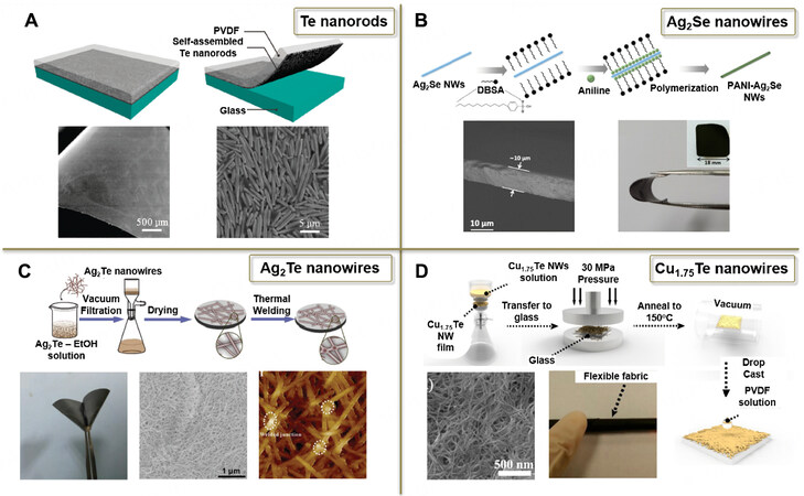
Figure 4. Synthesis of 1-Dimensional inorganic TE materials. (A) PVDF-Te nanorods composite films, adapted with permission from[55], (B) PANI-Ag2Se NW/PVDF films, adapted with permission from[56], (C) Ag2Te films, adapted with permission from[57], and (D)
Similar to inorganic TE materials, organic TE materials (e.g., carbon nanotubes (CNT) and
Synthesis methods for organic TE materials/films that are suitable for adaptation towards Materials Jetting of TE devices
| Method of fabrication | TE material | Additives | Thermal conductivity (W/mK) | Seebeck coefficient (µV/K) | Electrical conductivity (S/cm) | Power factor (µW/mK2) | zTat room temp. | Ref. |
| Bar Coating | PEDOT:PSS, Graphene, CNT | - | 0.36 | 23.2 | 689 | 37.08 | 0.031 | [59] |
| Casting | CNT | PVA emulsion | 0.34 | 38 | 48 | 6.9 | 0.006 | [60] |
| Casting | SWCNT, PEDOT:PSS | - | 0.2-0.4 | 18.3 | 400 | 13.4 | 0.02 | [61] |
| Casting | SWCNT, Polyaniline (PANI) | - | 0.43 | 65 | 769 | 176 | 0.12 | [62] |
| Drop Casting | CNT | Benzyl viologen | 5 | -116 | 1534 | 3103 | 0.20 | [63] |
| Drop Casting (50 % CNT composite film) | SWCNT | Poly[N-butyl-2-[5,5'-(2,5-bis(octyloxy)-1,4-phenylene)bis(thiophene-2-yl)vinyl]pyridinium iodide] | - | 54 | 159 | 46.4 | - | [64] |
| Drop Casting | DWCNT, Polyaniline | Camphorsulfonic acid | - | 61 | 610 | 220 | - | [65] |
| Drop Casting | SWCNT, PEDOT:PSS | DMSO | 0.4-0.6 | 55.6 | 1701 | 526 | 0.39 | [66] |
| Drop Casting (6.7 wt % CNT) | PEDOT:PSS, SWCNT | Formic acid | - | 54 | 1300 | 407 | - | [67] |
| Drop Casting (6.7 wt% CNT) | PEDOT:PSS, SWCNT | DMSO | - | 59 | 1230 | 464 | - | [67] |
| Floating-Catalyst Chemical Vapor Deposition | CNT, PEDOT:PSS | - | - | 82.9 | 734.5 | 504.8 | - | [68] |
| Spray Coating | SWCNT | PEI | - | -58 | 10 | 3.4 | - | [69] |
| Spray Coating | SWCNT, Poly(3,4-ethylenedioxythiophene) (PEDOT) | Tetrakis(dimethylamino)ethylene | 0.67 | -1250 | 6.6 | 1050 | 0.5 | [70] |
| Vacuum Filtration | DWCNT | Chlorosulfonic acid | - | 18 | 17,400 | 550.8 | - | [71] |
| Vacuum Filtration | SWCNT | Napthalene diimide | - | -55 | 446 | 135 | - | [72] |
| Vacuum Filtration | SWCNT | Perylene diimide | - | -47.3 | 500 | 112 | - | [72] |
| Vacuum Filtration | SWCNT | Poly-Schiff base | - | 42.7-44.1 | 393-430 | 71.9-83.5 | - | [73] |
| Vacuum Filtration | SWCNT, Poly(3,4-ethylenedioxythiophene) (PEDOT:PF6) | - | - | 51.0-56.8 | 1357-1531 | 243.3-264.1 | - | [74] |
| Vacuum Filtration (70 wt% SWCNT) | SWCNT, PEDOT:PSS coated Te nanorod | H2SO4 | - | 56 | 332 | 104 | - | [75] |
| Wet Spinning | SWCNT, PEDOT:PSS | - | 0.71 | 35 | 980 | 83.5 | 0.035 | [76] |
| Wet Spinning | SWCNT, PEDOT:PSS | PEI | 0.39 | -48.2 | 540 | 126 | 0.096 | [76] |
Materials-jetted thermoelectrics
Individual merits of organic, inorganic, and composite TE materials have garnered considerable attention in the TE community. While these materials have been explored in bulk and thin film forms, interest has been growing, particularly for TE devices fabricated via 3D printing. 3D printing offers the capabilities of multi-material printing for TE device fabrication. Research efforts have been channeled towards optimizing the printability of flexible, conformable devices while sustaining modest TE performance. However, not much research has been done in this field of Materials Jetted TE to date. The reported literature on materials jetted TE materials are tabulated in Table 3.
3D printed TE materials fabricated via Materials Jetting
| Method of fabrication | TE material | Additives | Thermal conductivity (W/mK) | Seebeck coefficient (µV/K) | Electrical conductivity (S/cm) | Power factor (µW/mK2) | zT | Ref. |
| Organic and Composites | ||||||||
| Aerosol Jetting | Bi2Te3- PEDOT:PSS | EG, water | - | 22.5 | 360 | ~18 | - | [81] |
| Aerosol Jetting | Sb2Te3 - PEDOT:PSS | EG, water | - | 33.8 | 247.3 | 28.3 | - | [81] |
| Aerosol Jetting | Sb2Te3-MWCNTs-PEDOT:PSS | PVP, water | - | 29 | 496 | 41 | - | [82] |
| Inkjet Printing | (PEDOT)xV2O5 | Triton X-100 | 0.68 | -350 | 0.16 | 2 | 0.001 | [83] |
| Inkjet Printing | Poly[Cux(Cu-ett)] | PVDF, DMSO | - | 41 | 5.14 | 0.86 | - | [84] |
| Inkjet Printing | Poly[Kx(Ni-ett)] | PVDF, DMSO | - | -44.9 | 2.12 | 0.43 | - | [84] |
| Inkjet Printing | Graphene | PVP, IPA | - | 41 | - | 18.7 | - | [85] |
| Inorganic | ||||||||
| Inkjet Printing | Bi2Te3 NW | Water | 0.193 | -94.2 | 172.6 | 163 | 0.26 | [86] |
| Inkjet Printing | Bi0.5Sb1.5Te3 NW | Water | 0.55 (in-plane) | 85.7 | 240.8 | 180 | 0.13 | [87] |
| Inkjet Printing | Bi2Te3 NW | Water | 1.19 (in-plane) | -117.2 | 82.0 | 110 | 0.04 | [87] |
Solution-based organic TE materials alleviate the chances for clogged prints and thus increase the success rate of printed TE devices. As evidenced by the ease of solution-based organic materials printing, there are more reports on organic and composite TE materials jetting[81-85] as compared to inorganic materials jetting[86,87] as shown in Table 3. For example, Juntunen and colleagues synthesized graphene films exhibiting a room temperature Seebeck of 41 μV/K and a power factor of 18.7 μW/mK2, which is comparable to existing graphene-conductive polymer nanocomposites [Figure 5A][85]. A room temperature charge carrier concentration of 3.17 × 1019 cm-3 and a hole mobility of 21.5 cm2/Vs were also achieved. The carrier concentration value agrees with their proposed model that the films exhibited electrical transport behavior from the few-layer graphene flakes and were not influenced by the disordered structure of the film. The fabrication process via the incorporation of minute amounts of polyvinylpyrrolidone (PVP) into exfoliated graphite in IPA resulted in a well-connected 3D network printable over a large area. The resultant film also proved to be stable after 10,000 bending repetitions over a 4.5 mm radius. Similarly, in Figure 5B, Ferhat and colleagues[83] utilized inkjet printing for vanadium pentoxide (V2O5) xerogels incorporated with
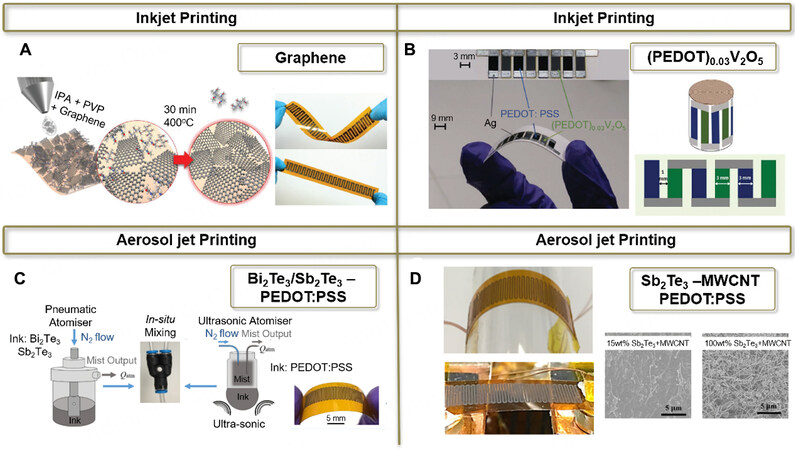
In addition to inkjet printing, aerosol jet printing is also being explored in fabricating printed composite-based thermoelectric devices. In Figure 5C, Ou and colleagues[81] reported a PEDOT:PSS matrix mixed with Bi2Te3/Sb2Te3 nanoparticles to enhance the electrical transport. The incorporation of 85 wt% Sb2Te3 nanoflakes resulted in a Seebeck coefficient of 33.8 μV/K, and an electrical conductivity of 247.3 S/cm, ultimately demonstrating a peak power factor of 28.3 μW/mK2. In their later study, Ou’s group explored the addition of multi-walled carbon nanotubes (MWCNT) and Sb2Te3 in PEDOT:PSS and similarly found that 85 wt% loading of Sb2Te3 and MWCNT yielded a further improvement with a power factor of
From Table 3, inorganic TE NWs are promising materials to be jetted, yet there have not been many studies in this area. A study done by Chen and colleagues demonstrated the successful ink jetting of synthesized singly crystalline Bi2Te3 NWs[86]. The Bi2Te3 NWs achieved a power factor of 163 μW/mK2 and zT of 0.26 at room temperature. For the second study, the same group achieved a high power factor of 180 μW/mK2 at 400 K for Bi0.5Sb1.5Te3 NWs and 110 μW/mK2 at the same temperature was obtained for the Bi2Te3 NWs[87]. Synthesized NWs were ink jetted onto a flexible polyimide substrate and a flexible thin-film TEG device, made up of 5 pairs of Bi2Te3 and Bi0.5Sb1.5Te3 NWs, was fabricated. An output voltage of 45 mV was achieved at a temperature difference of 32.5 K for the device. The zT performance of the reported jetted inorganic TE materials is at least two orders of magnitude higher than the materials jetted organic TE materials, as shown in Table 3. Despite these efforts, current materials jetted TE materials performance still pales in comparison to conventional spark plasma sintered or hot pressed TE materials[88-90]. Nonetheless, these studies suggest that MJ has high potential as a viable fabrication approach for flexible thermoelectric applications and should be further explored.
Ink properties for materials-jetted thermoelectrics
To improve the current state of Materials Jetted TE technology, the necessary ink properties and printing parameters for a successful print must be well understood. Here, two ink properties - flow behavior and material curing will be discussed. Optimization of printing parameters such as the speed of jetting, input pressure, nozzle dwell time (pulse width) and number of repetitions are discussed in other papers[91,92]. The substrate property (i.e., porosity and surface tension) is also an important factor to be considered and has also been detailed in other papers[93,94].
First, the TE ink needs to have an optimal flow behavior. For Newtonian fluids, droplet formation is determined by the dimensionless inverse (Z) of the Ohnesorge number (Oh) which is related to the Reynolds (Re) and Weber (We) numbers. The inverse of the Ohnesorge number is given by
Second, most MJ inks are water/solvent-based systems, and the primary mode of curing is through solvent evaporation. The solvent drying conditions are essential in controlling the printed morphology and microstructural porosity, and particle arrangement. The formation of “coffee rings” happens when ink is left to dry on the substrate. The phenomenon happens when solvent evaporation drives an outward radial flow, transporting material towards the periphery, causing defects and poor structural resolution[98]. To minimize the formation of “coffee rings” of ink jetted graphene oxide, Derby and He developed a model to understand the influence of substrate bed temperature, graphene oxide particle size and droplet size on the solvent evaporation[98]. Apart from controlling these parameters, adding cosolvents [such as sodium dodecyl sulfate (SDS)] changes the surface tension to promote an opposing Marangoni flow and can also alleviate “coffee ring” defects[99]. However, “offee rings” may still have their merits, particularly in the field of printed electronics. Due to the strong wettability contrast between the surface-modified hydrophobic and hydrophilic substrate regions, Takenobu and colleagues achieved highly aligned ink jetted single-walled carbon nanotubes for high-performance electronic devices[100]. In a similar vein, as shown in
CONCLUSION AND OUTLOOK
Thermoelectrics is an attractive class of material for energy harvesting and cooling technology. Particularly, thermoelectrics has garnered renewed interest as an energy harvesting material for waste heat recovery from body heat to exhaust systems. Its direct conversion from waste heat into useful electrical energy allows it to be implemented in many waste heat systems. However, due to the high processing and material cost, thermoelectrics is still limited to niche applications for remote powering in military and spacecraft systems[102]. Additive manufacturing technology, however, offers cost-effective manufacturing of thermoelectrics for industrial and wearable energy harvesting applications. The growing trend beyond conventional vertical and planar thermoelectric designs towards complex configurations for efficient heat conversion can be easily realized with additive manufacturing. Specifically, materials jetting is a fitting pillar of additive manufacturing that is well-suited for 3D printing of electronics. This facile and relatively cheap printing technique offers the advantages of multi-material printing for device fabrication with minimal inter-material delamination, thus allowing for the large-scale fabrication and automation of TE device manufacturing. The ability for substrate-based printing of two-dimensional thermoelectrics allows the flexible device to conform to host pipes and human wrists for waste heat conversion. However, with any substrate-based system, the working temperature of the printed device is limited by the substrate working temperature. Often, these are textile substrates with low degradation temperatures. Therefore, alternative substrates such as metal and ceramic for high temperature applications should be explored. Consequently, 5-axis 3D printers can also be considered for 3D conformal electronics. With the limited number of elemental semiconductors such as Te, Ge and Ga, conjugated polymers and carbon-based materials should be studied to create an impact in the long term using cost-effective and sustainable raw materials. However, with the lower zT performance of organic TE materials, research developments in the areas of chemical functionalization, composites and nano-structuring are required to make organic TE materials feasible for large-scale employment. The complex morphology of organic materials at the nanoscale brings high potential for achieving high zT through nano-structuring. Materials jetting of 1D materials will thus add value to the thermoelectric performance by tailoring the microstructural architecture. Therefore, if fully embraced, materials jetting of thermoelectrics would be a feasible pathway towards efficient self-powered TE devices.
DECLARATIONS
Authors’ contributionsConceptualization and writing: Zhang D
Writing: Sia SA, Solco SFD
Supervision and writing: Xu J, Suwardi A
Availability of data and materialsNot applicable.
Financial support and sponsorshipThis work was supported by A*STAR, Singapore Career Development Fund (CDF) C210112022 and
All authors declared that there are no conflicts of interest.
Ethical approval and consent to participateNot applicable.
Consent for publicationNot applicable.
Copyright© The Author(s) 2023.
REFERENCES
1. Johnson I, Choate WT, Davidson A. Waste heat recovery. In technology and opportunities in US industry. Laurel, MD: BCS, Inc.; 2008. Available from: https://www1.eere.energy.gov/manufacturing/intensiveprocesses/pdfs/waste_heat_recovery.pdf [Last accessed on 6 Jan 2023].
2. Farhat O, Faraj J, Hachem F, Castelain C, Khaled M. A recent review on waste heat recovery methodologies and applications: comprehensive review, critical analysis and potential recommendations. Clean Eng Technol 2022;6:100387.
3. Energy DO. Industrial heat pumps for steam and fuel saving 2014. Available from: https://www.energy.gov/sites/prod/files/2014/05/f15/heatpump.pdf [Last accessed on 6 Jan 2023].
4. Wang N, Ni L, Wang A, Shan H, Jia H, Zuo L. High-efficiency photovoltaic-thermoelectric hybrid energy harvesting system based on functionally multiplexed intelligent thermal management. Energy Convers Manag 2022;272:116377.
5. Wang N, Gao C, Ding C, Jia H, Sui G, Gao X. A thermal management system to reuse thermal waste released by high-power light-emitting diodes. IEEE Trans Electron Devices 2019;66:4790-7.
6. Wang Y, Shi Y, Mei D, Chen Z. Wearable thermoelectric generator for harvesting heat on the curved human wrist. Appl Energy 2017;205:710-9.
7. Ren W, Sun Y, Zhao D, et al. High-performance wearable thermoelectric generator with self-healing, recycling, and Lego-like reconfiguring capabilities. Sci Adv 2021;7:eabe0586.
8. Kim CS, Yang HM, Lee J, et al. Self-powered wearable electrocardiography using a wearable thermoelectric power generator. ACS Energy Lett 2018;3:501-7.
9. Deng W, Deng L, Hu Y, Zhang Y, Chen G. Thermoelectric and mechanical performances of ionic liquid-modulated PEDOT:PSS/SWCNT composites at high temperatures. Soft Sci 2022;1:14.
10. Zou Q, Shang H, Huang D, et al. Improved thermoelectric performance in n-type flexible Bi2Se3+x/PVDF composite films. Soft Sci 2021;1:2.
11. Satoh N, Otsuka M, Kawakita J, Mori T. A hierarchical design for thermoelectric hybrid materials: Bi2Te3 particles covered by partial Au skins enhance thermoelectric performance in sticky thermoelectric materials. Soft Sci 2022;2:15.
12. Cao J, Zheng J, Liu H, et al. Flexible elemental thermoelectrics with ultra-high power density. Mater Today Energy 2022;25:100964.
13. Jia N, Cao J, Tan XY, et al. Suppressing Ge-vacancies to achieve high single-leg efficiency in GeTe with an ultra-high room temperature power factor. J Mater Chem A 2021;9:23335-44.
14. Suwardi A, Cao J, Zhao Y, et al. Achieving high thermoelectric quality factor toward high figure of merit in GeTe. Mater Today Phys 2020;14:100239.
15. Mao J, Zhu H, Ding Z, et al. High thermoelectric cooling performance of n-type Mg3Bi2-based materials. Science 2019;365:495-8.
16. Chen C, Shen D, Xia C, et al. Integrating band engineering with point defect scattering for high thermoelectric performance in Bi2Si2Te6. Chem Eng J 2022;441:135968.
17. Pei Y, Zheng L, Li W, et al. Interstitial point defect scattering contributing to high thermoelectric performance in SnTe. Adv Electron Mater 2016;2:1600019.
18. Liang G, Zheng Z, Li F, et al. Nano structure Ti-doped skutterudite CoSb3 thin films through layer inter-diffusion for enhanced thermoelectric properties. J Eur Ceram Soc 2019;39:4842-9.
19. Wu H, Lu X, Wang G, et al. Strong lattice anharmonicity securing intrinsically low lattice thermal conductivity and high performance thermoelectric SnSb2Te4 via Se alloying. Nano Energy 2020;76:105084.
20. Abbas FI, Yamashita A, Hoshi K, et al. Investigation of lattice anharmonicity in thermoelectric LaOBiS2-xSex through Grüneisen parameter. Appl Phys Express 2021;14:071002.
21. Jia N, Cao J, Tan XY, et al. Thermoelectric materials and transport physics. Mater Today Phys 2021;21:100519.
22. Zhang D, Lim WYS, Duran SSF, Loh XJ, Suwardi A. Additive Manufacturing of thermoelectrics: emerging trends and outlook. ACS Energy Lett 2022;7:720-35.
23. Zhu Q, Wang S, Wang X, et al. Bottom-up engineering strategies for high-performance thermoelectric materials. Nanomicro Lett 2021;13:119.
24. Zhuang H, Pei J, Cai B, et al. Thermoelectric performance enhancement in BiSbTe alloy by microstructure modulation via cyclic spark plasma sintering with liquid phase. Adv Funct Mater 2021;31:2009681.
25. Cai B, Zhuang H, Pei J, et al. Spark plasma sintered Bi-Sb-Te alloys derived from ingot scrap: maximizing thermoelectric performance by tailoring their composition and optimizing sintering time. Nano Energy 2021;85:106040.
26. Xin N, Li Y, Shen H, Shen L, Tang G. Realizing high thermoelectric performance in hot-pressed polycrystalline AlxSn1-xSe through band engineering tuning. J Materiomics 2022;8:475-88.
27. Sturm C, Boccalon N, Assoud A, Zou T, Kycia J, Kleinke H. Thermoelectric properties of hot-pressed Ba3Cu14-δTe12. Inorg Chem 2021;60:12781-9.
28. Leonov V. Thermoelectric energy harvesting of human body heat for wearable sensors. IEEE Sensors J 2013;13:2284-91.
29. Kumar S, Gupta A, Yadav G, Singh HP. Peltier module for refrigeration and heating using embedded system, In 2015 international conference on recent developments in control, Automation and Power Engineering (RDCAPE), Noida, India, 12-13 March 2015; pp. 314-9.
30. Chang P, Liao C. Screen-printed flexible thermoelectric generator with directional heat collection design. J Alloys Compd 2020;836:155471.
31. Cao Z, Koukharenko E, Tudor M, Torah R, Beeby S. Flexible screen printed thermoelectric generator with enhanced processes and materials. Sensors Actuat A Phys 2016;238:196-206.
32. Pelegrini S, Adami A, Collini C, et al. In simulation, design and fabrication of a planar micro thermoelectric generator, smart sensors, actuators, and MEMS VI. SPIE; 2013; pp. 519-26.
33. Lourdes Gonzalez-juarez M, Flores E, Martin-gonzalez M, Nandhakumar I, Bradshaw D. Electrochemical deposition and thermoelectric characterisation of a semiconducting 2-D metal-organic framework thin film. J Mater Chem A 2020;8:13197-206.
34. Shen H, Lee H, Han S. Optimization and fabrication of a planar thermoelectric generator for a high-performance solar thermoelectric generator. Curr Appl Phys 2021;22:6-13.
35. Goncalves LM, Rocha JG, Couto C, et al. Fabrication of flexible thermoelectric microcoolers using planar thin-film technologies. J Micromech Microeng 2007;17:S168-73.
36. Kogo G, Xiao B, Danquah S, et al. A thin film efficient pn-junction thermoelectric device fabricated by self-align shadow mask. Sci Rep 2020;10:1067.
37. Junlabhut P, Nuthongkum P, Sakulkalavek A, Harnwunggmoung A, Limsuwan P, Sakdanuphab R. Enhancing the thermoelectric properties of sputtered Sb2Te3 thick films via post-annealing treatment. Surf Coat Technol 2020;387:125510.
38. Owoyele O, Ferguson S, O’connor BT. Performance analysis of a thermoelectric cooler with a corrugated architecture. Appl Energy 2015;147:184-91.
39. Rösch AG, Gall A, Aslan S, et al. Fully printed origami thermoelectric generators for energy-harvesting. NPJ Flex Electron 2021:5.
40. Huu T, Nguyen Van T, Takahito O. Flexible thermoelectric power generator with Y-type structure using electrochemical deposition process. Appl Energy 2018;210:467-76.
41. Sun T, Zhou B, Zheng Q, Wang L, Jiang W, Snyder GJ. Stretchable fabric generates electric power from woven thermoelectric fibers. Nat Commun 2020;11:572.
42. Andjela L, Abdurahmanovich VM, Vladimirovna SN, Mikhailovna GI, Yurievich DD, Alekseevna MY. A review on vat photopolymerization 3D-printing processes for dental application. Dent Mater 2022;38:e284-96.
43. Methani MM, Cesar PF, de Paula Miranda RB, Morimoto S, Özcan M, Revilla-león M. Additive manufacturing in dentistry: current technologies, clinical applications, and limitations. Curr Oral Health Rep 2020;7:327-34.
44. Najmon JC, Raeisi S, Tovar A. Review of additive manufacturing technologies and applications in the aerospace industry. In Additive manufacturing for the aerospace industry. 2019; pp. 7-31.
45. Kim F, Yang SE, Ju H, et al. Direct ink writing of three-dimensional thermoelectric microarchitectures. Nat Electron 2021;4:579-87.
46. Su N, Zhu P, Pan Y, Li F, Li B. 3D-printing of shape-controllable thermoelectric devices with enhanced output performance. Energy 2020;195:116892.
47. Yang SE, Kim F, Ejaz F, et al. Composition-segmented BiSbTe thermoelectric generator fabricated by multimaterial 3D printing. Nano Energy 2021;81:105638.
48. Stratasys PolyJet. Available from: https://www.stratasys.com/en/3d-printers/printer-catalog/polyjet/?filter=PolyJet [Last accessed on 6 Jan 2023].
49. Optomec aerosol jet technology. Available from: https://optomec.com/printed-electronics/aerosol-jet-technology/ [Last accessed on 6 Jan 2023].
50. Hoath SD. Fundamentals of inkjet printing: the science of inkjet and droplets. Hoboken, NJ: John Wiley & Sons; 2016.
51. Zhao D, Zhou H, Wang Y, Yin J, Huang Y. Drop-on-demand (DOD) inkjet dynamics of printing viscoelastic conductive ink. Addit Manuf 2021;48:102451.
52. Xu X, Yang J, Jonhson W, et al. Additive manufacturing solidification methodologies for ink formulation. Addit Manuf 2022;56:102939.
53. Fathi S, Dickens P. Jettability of reactive nylon materials for additive manufacturing applications. J Manuf Process 2012;14:403-13.
54. Agarwala S, Goh GL, Yeong WY. Optimizing aerosol jet printing process of silver ink for printed electronics, In IOP Conference series: materials science and engineering; 2017; p. 012027.
55. Dun C, Hewitt CA, Huang H, Montgomery DS, Xu J, Carroll DL. Flexible thermoelectric fabrics based on self-assembled tellurium nanorods with a large power factor. Phys Chem Chem Phys 2015;17:8591-5.
56. Park D, Kim M, Kim J. High-performance PANI-coated Ag2Se nanowire and PVDF thermoelectric composite film for flexible energy harvesting. J Alloys Compd 2021;884:161098.
57. Zeng X, Yan C, Ren L, et al. Silver telluride nanowire assembly for high-performance flexible thermoelectric film and its application in self-powered temperature sensor. Adv Electron Mater 2019;5:1800612.
58. Zhou C, Dun C, Wang Q, et al. Nanowires as building blocks to fabricate flexible thermoelectric fabric: the case of copper telluride nanowires. ACS Appl Mater Interfaces 2015;7:21015-20.
59. Yoo D, Kim J, Lee SH, et al. Effects of one- and two-dimensional carbon hybridization of PEDOT:PSS on the power factor of polymer thermoelectric energy conversion devices. J Mater Chem A 2015;3:6526-33.
60. Yu C, Kim YS, Kim D, Grunlan JC. Thermoelectric behavior of segregated-network polymer nanocomposites. Nano Lett 2008;8:4428-32.
61. Kim D, Kim Y, Choi K, Grunlan JC, Yu C. Improved thermoelectric behavior of nanotube-filled polymer composites with
62. Yao Q, Wang Q, Wang L, Chen L. Abnormally enhanced thermoelectric transport properties of SWNT/PANI hybrid films by the strengthened PANI molecular ordering. Energy Environ Sci 2014;7:3801-7.
63. An CJ, Kang YH, Song H, Jeong Y, Cho SY. High-performance flexible thermoelectric generator by control of electronic structure of directly spun carbon nanotube webs with various molecular dopants. J Mater Chem A 2017;5:15631-9.
64. Qu S, Yao Q, Wang L, Hua J, Chen L. A novel hydrophilic pyridinium salt polymer/SWCNTs composite film for high thermoelectric performance. Polymer 2018;136:149-56.
65. Wang H, Yi SI, Pu X, Yu C. Simultaneously improving electrical conductivity and thermopower of polyaniline composites by utilizing carbon nanotubes as high mobility conduits. ACS Appl Mater Interfaces 2015;7:9589-97.
66. Liu S, Li H, He C. Simultaneous enhancement of electrical conductivity and seebeck coefficient in organic thermoelectric SWNT/PEDOT:PSS nanocomposites. Carbon 2019;149:25-32.
67. Hsu J, Choi W, Yang G, Yu C. Origin of unusual thermoelectric transport behaviors in carbon nanotube filled polymer composites after solvent/acid treatments. Org Electron 2017;45:182-9.
68. Li D, Luo C, Chen Y, et al. High performance polymer thermoelectric composite achieved by carbon-coated carbon nanotubes network. ACS Appl Energy Mater 2019;2:2427-34.
69. Ryu Y, Freeman D, Yu C. High electrical conductivity and n-type thermopower from double-/single-wall carbon nanotubes by manipulating charge interactions between nanotubes and organic/inorganic nanomaterials. Carbon 2011;49:4745-51.
70. Wang H, Hsu JH, Yi SI, et al. Thermally driven large N-type voltage responses from hybrids of carbon nanotubes and poly(3,4-ethylenedioxythiophene) with tetrakis(dimethylamino)ethylene. Adv Mater 2015;27:6855-61.
71. Ryu Y, Yin L, Yu C. Dramatic electrical conductivity improvement of carbon nanotube networks by simultaneous de-bundling and hole-doping with chlorosulfonic acid. J Mater Chem 2012;22:6959.
72. Wu G, Zhang ZG, Li Y, Gao C, Wang X, Chen G. Exploring high-performance n-type thermoelectric composites using amino-substituted rylene dimides and carbon nanotubes. ACS Nano 2017;11:5746-52.
73. Gao C, Chen G. A new strategy to construct thermoelectric composites of SWCNTs and poly-schiff bases with 1,4-diazabuta-1,3-diene structures acting as bidentate-chelating units. J Mater Chem A 2016;4:11299-306.
74. Fan W, Guo C, Chen G. Flexible films of poly(3,4-ethylenedioxythiophene)/carbon nanotube thermoelectric composites prepared by dynamic 3-phase interfacial electropolymerization and subsequent physical mixing. J Mater Chem A 2018;6:12275-80.
75. Meng Q, Cai K, Du Y, Chen L. Preparation and thermoelectric properties of SWCNT/PEDOT:PSS coated tellurium nanorod composite films. J Alloys Compd 2019;778:163-9.
76. Kim J, Lee W, Kang YH, Cho SY, Jang K. Wet-spinning and post-treatment of CNT/PEDOT:PSS composites for use in organic fiber-based thermoelectric generators. Carbon 2018;133:293-9.
77. Zhu B, Liu X, Wang Q, et al. Realizing record high performance in n-type Bi2Te3-based thermoelectric materials. Energy Environ Sci 2020;13:2106-14.
78. Zhao W, Fan S, Xiao N, et al. Flexible carbon nanotube papers with improved thermoelectric properties. Energy Environ Sci 2012;5:5364-9.
79. Yao CJ, Zhang HL, Zhang Q. Recent progress in thermoelectric materials based on conjugated polymers. Polymers 2019;11:107.
80. Zhang Y, Zhang Q, Chen G. Carbon and carbon composites for thermoelectric applications. Carbon Energy 2020;2:408-36.
81. Ou C, Sangle AL, Datta A, et al. Fully printed organic-inorganic nanocomposites for flexible thermoelectric applications. ACS Appl Mater Interfaces 2018;10:19580-7.
82. Ou C, Sangle AL, Chalklen T, Jing Q, Narayan V, Kar-narayan S. Enhanced thermoelectric properties of flexible aerosol-jet printed carbon nanotube-based nanocomposites. APL Mater 2018;6:096101.
83. Ferhat S, Domain C, Vidal J, Noël D, Ratier B, Lucas B. Organic thermoelectric devices based on a stable n-type nanocomposite printed on paper. Sustain Energy Fuels 2018;2:199-208.
84. Jiao F, Di CA, Sun Y, Sheng P, Xu W, Zhu D. Inkjet-printed flexible organic thin-film thermoelectric devices based on p- and n-type poly(metal 1,1,2,2-ethenetetrathiolate)s/polymer composites through ball-milling. Philos Trans Royal Soc A Math Phys Eng Sci 2014;372:20130008.
85. Juntunen T, Jussila H, Ruoho M, et al. Inkjet printed large-area flexible few-layer graphene thermoelectrics. Adv Funct Mater 2018;28:1800480.
86. Chen B, Das SR, Zheng W, et al. Inkjet printing of single-crystalline Bi2Te3 thermoelectric nanowire networks. Adv Electron Mater 2017;3:1600524.
87. Chen B, Kruse M, Xu B, et al. Flexible thermoelectric generators with inkjet-printed bismuth telluride nanowires and liquid metal contacts. Nanoscale 2019;11:5222-30.
88. Wang Y, Liu WD, Gao H, et al. High porosity in nanostructured n-Type Bi2Te3 obtaining ultralow lattice thermal conductivity. ACS Appl Mater Interfaces 2019;11:31237-44.
89. Finefrock SW, Zhang G, Bahk JH, et al. Structure and thermoelectric properties of spark plasma sintered ultrathin PbTe nanowires. Nano Lett 2014;14:3466-73.
90. Cao J, Tan XY, Jia N, et al. Designing good compatibility factor in segmented Bi0.5Sb1.5Te3-GeTe thermoelectrics for high power conversion efficiency. Nano Energy 2022;96:107147.
91. Lee A, Sudau K, Ahn KH, Lee SJ, Willenbacher N. Optimization of experimental parameters to suppress nozzle clogging in inkjet printing. Ind Eng Chem Res 2012;51:13195-204.
92. Liou T, Chan C, Shih K. Effects of actuating waveform, ink property, and nozzle size on piezoelectrically driven inkjet droplets. Microfluid Nanofluid 2010;8:575-86.
94. Krainer S, Smit C, Hirn U. The effect of viscosity and surface tension on inkjet printed picoliter dots. RSC Adv 2019;9:31708-19.
95. Jang D, Kim D, Moon J. Influence of fluid physical properties on ink-jet printability. Langmuir 2009;25:2629-35.
96. Zhang Y, Hu G, Liu Y, Wang J, Yang G, Li D. Suppression and utilization of satellite droplets for inkjet printing: a review. Processes 2022;10:932.
98. He P, Derby B. Controlling coffee ring formation during drying of inkjet printed 2D inks. Adv Mater Interfaces 2017;4:1700944.
99. Still T, Yunker PJ, Yodh AG. Surfactant-induced Marangoni eddies alter the coffee-rings of evaporating colloidal drops. Langmuir 2012;28:4984-8.
100. Takagi Y, Nobusa Y, Gocho S, et al. Inkjet printing of aligned single-walled carbon-nanotube thin films. Appl Phys Lett 2013;102:143107.
101. Goh GL, Agarwala S, Yeong WY. Aerosol-jet-printed preferentially aligned carbon nanotube twin-lines for printed electronics. ACS Appl Mater Interfaces 2019;11:43719-30.
Cite This Article
Export citation file: BibTeX | RIS
OAE Style
Zhang D, Sia SA, Solco SFD, Xu J, Suwardi A. Energy harvesting through thermoelectrics: topological designs and materials jetting technology. Soft Sci 2023;3:1. http://dx.doi.org/10.20517/ss.2022.29
AMA Style
Zhang D, Sia SA, Solco SFD, Xu J, Suwardi A. Energy harvesting through thermoelectrics: topological designs and materials jetting technology. Soft Science. 2023; 3(1): 1. http://dx.doi.org/10.20517/ss.2022.29
Chicago/Turabian Style
Zhang, Danwei, Seng Ann Sia, Samantha Faye Duran Solco, Jianwei Xu, Ady Suwardi. 2023. "Energy harvesting through thermoelectrics: topological designs and materials jetting technology" Soft Science. 3, no.1: 1. http://dx.doi.org/10.20517/ss.2022.29
ACS Style
Zhang, D.; Sia SA.; Solco SFD.; Xu J.; Suwardi A. Energy harvesting through thermoelectrics: topological designs and materials jetting technology. Soft. Sci. 2023, 3, 1. http://dx.doi.org/10.20517/ss.2022.29
About This Article
Copyright

Data & Comments
Data


 Cite This Article 21 clicks

 Like This Article 29
likes
Like This Article 29
likes


Comments
Comments must be written in English. Spam, offensive content, impersonation, and private information will not be permitted. If any comment is reported and identified as inappropriate content by OAE staff, the comment will be removed without notice. If you have any queries or need any help, please contact us at support@oaepublish.com.