
Direct fabrication of high-performance multi-response e-skin based on a graphene nanosheet film


Abstract
With the increasing popularity of wearable devices, lightweight electronic skin (e-skin) has attracted significant attention. However, current fabrication technologies make it difficult to directly fabricate sensing materials on flexible substrates at low temperatures. Hence, we propose a flexible graphene nanosheet-embedded carbon
Keywords
INTRODUCTION
In recent years, wearable electronic device technology has been used in a wide range of applications in motion detection[1-5], medical monitoring[6-9] and virtual reality (VR)[10-12]. In particular, electronic skin
Carbon-based materials, such as carbon nanotubes (CNTs)[29,32-35] and graphene[36], are widely used in flexible sensors due to their exotic properties. For example, Zhao et al. prepared a flexible sensor based on multi-walled CNTs and polyaniline, which could detect body movement through triboelectricity[37]. Qiao et al. used silver nanowires to bridge and laser scribe graphene oxide to obtain a new type of e-skin that could detect small movements, such as the human pulse and respiration[38]. Zhu et al. used a mixture of graphene and Ag powder with organic glue as a functional material to fabricate a multi-field sensing grab manipulator using mask printing[31]. Moreover, to improve the sensitivity of carbon-based e-skin to construct microstructures, researchers proposed a lot of methods such as serpentine[39], sponge[40,41] and wave structures[19,33]. At present, large single-crystal graphene or high-quality CNTs are usually prepared by chemical vapor deposition (CVD) at high temperatures. For example, Pan et al. proposed high-sensitivity strain sensors based on a three-dimensional (3D) graphene film, firstly grown by CVD at 1000 °C, on polydimethylsiloxane[42]. Hence, current technologies generally adopt the multi-step method of first preparing, then peeling off and finally transferring the sensing material to the flexible substrate. Previous direct fabrication methods have mostly focused on nanodroplet or laser printing which have achieved considerable success in flexible printing devices. Although expensive for single fabrications, vacuum fabrication is widely adopted in industry due to its advantage in batch fabrications. Current vacuum batch fabrication technologies cannot be easily used to obtain wafer-level detectors by directly fabricating the sensing materials on flexible substrates at low temperatures.
On this basis, we propose an electron cyclotron resonance (ECR) low-temperature-sputtering system
EXPERIMENTAL
Direct preparation of F-GNEC film and e-skin structure
The F-GNEC film in this study is directly prepared using an ECR low-temperature sputtering system[45,51]
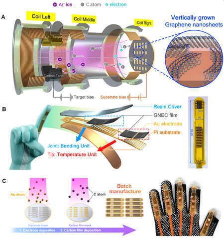
Figure 1. ECR system and overall manufacturing process of F-GNEC film sensor. (A) Schematic diagram of F-GNEC film prepared by ECR sputtering system, where the purple, gray and blue dots represent argon ions, carbon atoms and electrons, respectively. (B) Schematic diagram of F-GNEC-based e-skin and the specific structure design with the detection area divided as the finger structure so that the e-skin can realize multi-response detection and avoid interference. (C) Fabrication process of F-GNEC film-based e-skin, where the direct film preparation can effectively reduce defects and the simple and reliable preparation process is convenient for batch fabrication.
ECR low-temperature sputtering systems can directly fabricate devices on flexible substrates at low temperatures based on the unique plasma generation and polariton energy transfer modes of ECR. The ECR system uses microwaves to induce stable plasma and magnetic coils to accelerate the electrons and ions to sputter the target atoms. By applying a positive bias to the substrate, electrons are accelerated and collide with free carbon atoms. Therefore, the carbon atoms tend to bond as sp2 and the GNs grow vertically from the substrate. Hence, the generation of plasma and the sputtering process are independent in the ECR system, which is different from common sputtering systems where the generation of plasma is dependent on substrate bias. Based on this, the distance and heat transfer between the plasma and substrate can be modulated and controlled. The power of ECR plasma can be described as follows:

where c is the power coefficient, r is the plasma distance and B is the magnetic strength of the magnetic coils. Furthermore, the energy transfer mode between the plasma and substrate surface is not purely a thermal effect but a “low-temperature polariton” energy transfer mode [Supplementary Figure 2]. In short, the low-energy electrons in the ECR plasma interact with the lattice of the substrate surface to form polaritons. The polaritons repair the neighbor lattices to form sp2 bonds and release energy. This process can be described by the following Hamiltonians:
where Un is the coordinate of the atom core in the lattice, k is the Hamonic oscillation strength, Vn is the strength of the external field of the plasma and tn is the overlap integral of the electron clouds. Therefore, the internal temperature of the chamber is lower (125-175 °C), as measured by a vacuum infrared thermometer [Supplementary Figure 3].
By adjusting parameters, such as the gas flux, microwave power, substrate bias and deposition time during the film growth process, carbon films with different GN nanostructures can be prepared. Since the density of the GNs is related to the performance of the GNEC film, we can adjust the sensitivity or detection range depending on the requirements. The ECR system can also deposit up to three different substances in situ, which provides a convenient method for the synchronous manufacturing of electrodes and sensing structures. The maximum fabrication area is an 8-inch wafer, which allows for large-scale physical deposition.
A schematic diagram of e-skin based on the F-GNEC film is shown on the left side of Figure 1B. The e-skin is fixed on fingers to detect finger movement and temperature and optical signals. From bottom to top, there are the polyimide (PI) substrate, Au electrodes, F-GNEC film (with a thickness of ~100 nm) and a transparent resin encapsulation layer. The partial dimensions of the sensor are shown on the right side of Figure 1B. In order to avoid the interference of different signals, the sensor is designed as two independent parts, with an optical sensor at the fingertip and a bending sensor in the middle of the finger. To adapt to the different finger lengths of different users, the bending sensing part is designed as a long rectangular area and covered with a interdigital electrode to capture bending signals. Flexible PI films have reasonable flexibility and excellent thermal stability, thereby providing reliable substrates for F-GNEC films. To improve the efficiency of capturing signal current carriers, Au electrodes were devised with interdigital patterns with a 1 mm spacing at the joint area and a 0.5 mm spacing at the fingertip area. The F-GNEC films were designed as two separate rectangular areas to eliminate the disturbance among different signals, namely, a joint area of 20 mm2 × 6 mm2 and a fingertip area of 8 mm2 × 6 mm2. The joint area aims to measure the bending angle, while the fingertip area is used to measure temperature and optical signals. Using a transparent resin not only protects the F-GNEC film and electrodes but also avoids hindering the transmission of light, thereby ensuring the accuracy of photodetection.
The fabrication process is shown in Figure 1C, mainly consisting of two steps of physical deposition, both using a metal mask to form the required patterns. First, in the ECR sputtering system, Au atoms were deposited on the PI substrate. Subsequently, the F-GNEC film was grown directly on the PI substrate and Au electrodes. According to previous research, the pre-stretching of flexible substrates contributes to the density and size of the GNs, while a higher density of GNs leads to overall better performance of the
F-GNEC film preparation
In this work, the F-GNEC film is directly grown on the substrate and electrodes through the ECR system. A high-vacuum and clean environment is provided inside the system and the high-power microwaves can be used to excite argon to generate plasma (the purple part in Figure 1A). Under the induction of the magnetic coil, the movement of plasma and electrons is constrained. Under the attraction of a 500 V target bias voltage, electrons bombard the annular carbon or Au target, which sputter out the corresponding atoms. The carbon atoms gradually deposit on the flexible PI substrate and form the uniform amorphous carbon film, while the Au thin films can be used as electrodes. To fabricate the patterned film, the corresponding patterned mask is cleaned with acetone and attached to the substrate. The substrate and mask are then sent into the high-vacuum chamber of the ECR system. Under a vacuum of 2 × 10⁻⁴ Pa, high-flux argon gas is passed into the chamber and argon plasma is generated under the induction of a 300 mW microwave. Argon ions are used to bombard the surface of the coating for 3 min, which can effectively remove any residuals. The deposition time is controlled at 30 min to ensure that the thickness of the deposited flexible carbon film is consistent. During the deposition process, applying a 40 V positive bias to the substrate can attract electrons to bombard the carbon film and induce vertical growth of GNs inside the carbon film. By adjusting the substrate bias and other parameters, the density of the GNs inside the carbon film can be adjusted, thereby adjusting the performance of the F-GNEC film. After the deposition, the sample is naturally cooled in the chamber for 2 h and the F-GNEC film with multiple stimulus responses is obtained.
E-skin fabrication
Considering that a bent finger joint is more obvious and the fingertip is less deformed, the e-skin is divided into the bending sensing area at the joints and the light and temperature detection area at the fingertips. For the electrode preparation, the interdigital electrode mask was placed directly on the substrate and then put into the ECR system. A 100 nm Au layer is deposited on the substrate as electrodes. The F-GNEC film is then prepared on the substrate and the electrodes. After that, a protective layer needs to be prepared to encapsulate the F-GNEC film sensor, with a 6102 transparent resin, exhibiting both flexibility and mechanical strength, used as the protection layer. The 6102 resin and its curing agent are mixed in a ratio of 1:1.1 by weight and the mixture is fully stirred in a planetary mixer for 5 min. The mixture is then placed in a vacuum box for 20 min to remove bubbles. Finally, the mixture is coated on the surface of the F-GNEC film sensor, which is then placed in a vacuum heating box and kept at 100 °C for 1 h to obtain a dense transparent protective layer.
Characterization of F-GNEC film-based e-skin
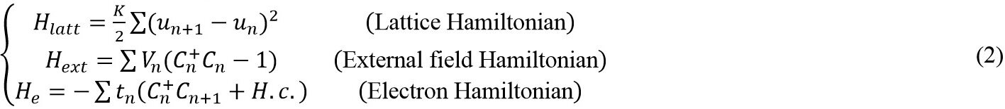
Transmission electron microscopy (TEM), atomic force microscopy (AFM) and Raman spectroscopy are used to analyze the size and distribution of the GNs and verify the preparation quality of the F-GNEC film. Figure 2A presents the TEM images of the standard F-GNEC and pre-stretching films under the same manufacturing parameters and the GNs are marked with white circles. It can be seen that the GNs are randomly distributed in the carbon film and form the conductive net. The inset presents the FFT image of the marked area and it can be seen that two clear Laue points appear. The reciprocal lattice distance
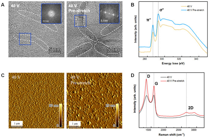
Figure 2. Characterization of F-GNEC films. (A) TEM images of standard and pre-stretching F-GNEC films. Insets show the FFT images of GNs. (B) Comparison of EELS spectra of standard and pre-stretching F-GNEC films. (C) AFM images of standard and pre-stretching F-GNEC films. (D) Comparison of Raman spectra of standard and pre-stretching F-GNEC films.
The surface morphologies of the F-GNEC films are shown in the AFM images in Figure 2C. Both the F-GNEC films show smooth surfaces with few scratches and cracks, which are conducive to the construction of a stable conductive network of GNs. It is obvious that the roughness of the pre-stretching F-GNEC film is much lower than the standard F-GNEC film. The Ra roughnesses are 24.3 and 35.4 nm, respectively, meaning that the pre-stretching process is beneficial for achieving lower roughness in the F-GNEC films.
Raman spectroscopy is essential for analyzing the bonding structure of the GNEC films. Since it is difficult to distinguish the Raman spectra of carbon films with the hinderance of the PI substrate, the F-GNEC films were scraped onto a SiO2 substrate. Figure 2D shows the Raman spectra of the standard and pre-stretching F-GNEC films ranging from 1100 to 2000 cm-1. It can be seen that each of the spectra shows a D peak near 1340 cm-1 and a G peak near 1590 cm-1, indicating ordered nanocrystalline structures. Unlike ideal graphene, the intensity of the D peak of the F-GNEC film is proportional to the probability of the formation of a carbon hexagonal ring, while the G peak arises due to the presence of sp2 carbon atoms in both the rings and chains. Hence, the high ratio of the D and G peaks (ID/IG) represents an sp2-hybridized long-range ordered structure, thereby proving the existence of GNs. Compared with the standard film, the pre-stretching film exhibits a higher ID/IG, indicating that it has a higher GN density.
Bending detection performance of F-GNEC film-based e-skin
The hand is one of the most important parts of the human body as it enables us to perform various complicated and subtle operations. Therefore, it is very important for e-skin to accurately and rapidly recognize its posture. Here, the F-GNEC film is attached to the finger joints and the bending of the finger joints produces tensile deformations in the F-GNEC film, causing a significant response
Figure 3. Stretching and bending test on F-GNEC film sensor. (A) Schematic diagram of the principle of tensile and bending detection of F-GNEC film. (B) Comparison of ΔR/R0 versus external tensile strains between the standard and pre-stretching films. (C) Specific ΔR/R0 versus external tensile strains and gauge factor of pre-stretching F-GNEC film. (D) Comparison of ΔR/R0 versus bending angles between the standard and pre-stretching film-based e-skin. (E) Multicycle bending of the pre-stretching F-GNEC film-based e-skin when bending at 30°, 60°, 90° and 120°. The inset depicts the response and recovery times under bending at 90°. (F) Multicycle bending of the pre-stretching F-GNEC film-based e-skin when bending at 90° with a frequency of 2, 1, 0.5 and 0.25Hz. (G) Stability and reliability test of pre-stretching F-GNEC film-based e-skin for 1000 bending 90° recovery cycles.
As shown in Figure 3B, the relative-resistance-change rate (ΔR/R0)-tensile strain (ε) curves of the standard and pre-stretching films are compared. When the tensile strain begins to increase, the ΔR/R0 of the standard F-GNEC film increases rapidly. When the ε increases to 30%, the ΔR/R0 reaches ~4 × 10⁵% and remains stable, meaning that the standard F-GNEC film is a completely open circuit. Additionally, the standard F-GNEC film has fewer GN edge wells and its resistance is smaller, resulting in a higher ΔR/R0 value in the open circuit. Since the pre-stretching F-GNEC film has a higher GN density, the conductive network is more stable. Although the ΔR/R0 of the pre-stretching F-GNEC film is lower, it has a wider measurement range, which can avoid the premature failure of the detector. The specific ΔR/R0-ε curve of the pre-stretching F-GNEC film is shown in Figure 3C, where the green and red curves represent the fitting lines of the low- and high-strain ranges, respectively. Here, the gauge factor (GF) is used to consider the sensitivity of the F-GNEC film and is defined as[59]:

In the range of 0%-4.32%, the tensile strain increases, the ΔR/R0 rapidly increases with the tensile strain and the GF value reaches the maximum value of 14,699 at ε = 0.5%. With a further increase in tensile strain, the pre-stretching F-GNEC film begins to stretch violently and its ΔR/R0 gradually increases. Owing to the local open circuit of the conductive network, the sensitivity of the F-GNEC film decreases. When ε = 100%, the ΔR/R0 reaches 343% and the GF value decreases to 817. Based on the sensitivity, the pre-stretching F-GNEC film e-skin can accurately measure the movement posture of the finger.
Figure 3D shows the ΔR/R0-bending angle (θ) curves of the pre-stretching F-GNEC film-based e-skin (red curve) and the standard F-GNEC film-based e-skin (black curve). It can be seen that when θ gradually increases from 0° to 90°, the ΔR/R0 of the pre-stretching F-GNEC film-based e-skin and the standard
Figure 3F shows the ΔR/R0 curves of the pre-stretching F-GNEC film-based e-skin when bent at 90° at frequencies of 2, 1, 0.5 and 0.25 Hz. It can be seen that the pre-stretching F-GNEC film-based e-skin can well capture high-frequency signals and the ΔR/R0 at each frequency remains stable. For wearable electronics, life span is also an important performance. As shown in Figure 3G, the pre-stretching F-GNEC film-based e-skin is bent at 90° 1000 times. The inset shows the ΔR/R0 curve of the first and last 50 bendings. After bending 1000 times, the ΔR/R0 of the F-GNEC film-based e-skin slightly reduced from 44.1% to 39.4%, showing outstanding stability and a long lifetime. Simultaneously, the ΔR/R0 of the standard F-GNEC film decreased from 32.8% to 26.8% [Supplementary Figure 3], indicating that the conductive network formed by high-density GNs is more stable. With the higher GN density, the pre-stretching F-GNEC film-based e-skin exhibits the advantages of excellent sensitivity, response speed and stability, thereby showing significant potential in VR and flexible robot applications.
Photodetection performance of F-GNEC film-based e-skin
The GNs in the GNEC film can be used as electron capture centers and play an important role in improving the photoelectric response. The principle of the F-GENC film-based e-skin to measure the optical signal is shown in Figure 4A, where the black hexagons and the blue dot represent GNs and electrons, respectively, while the yellow part represents the source and drain. In a dark environment, under the external bias voltage (Vsd), electrons will be separated from the edges of the GNs and attracted to the external circuit. Due to the edge quantum well of the GNs, the movement of electrons in the pre-stretched F-GNEC film is more difficult, so the dark current (Idark) is lower. Under laser irradiation, the electrons are excited from the valence band to the conduction band by the photons. Under the Vsd, the photogenerated electrons and holes are accelerated to separate, forming an outstanding photocurrent. Furthermore, the edges of the GNs capture a large number of photogenerated electrons and allow them to transport inside the GNs. The electrons in the F-GNEC film-based e-skin circulate continuously in capture and release so that the carrier life is improved. Therefore, the recombination rate of electron-hole pairs is greatly reduced, which effectively improves the photoelectric response and response speed of the F-GNEC film[36,45].
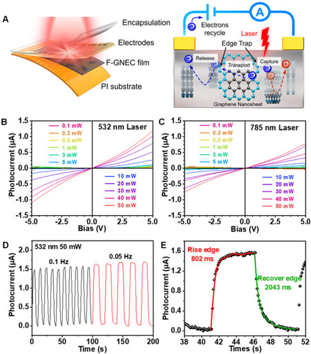
Figure 4. Photoelectric response of F-GNEC film sensor. (A) Schematic diagram of photodetection of F-GNEC film-based e-skin. Photocurrent-voltage (Iph-Vsd) curves of F-GNEC film-based e-skin at bias from -5 to 5 V under (B) a 532 nm laser and (C) a 785 nm laser with a laser power change from 0.1 to 50 mW. (D) Multicycle of laser ON/OFF of F-GNEC film-based e-skin under the 532 nm laser with frequencies of 0.1 and 0.05 Hz. (E) A single photoresponse under a 0.1 Hz laser exhibiting a response time of 802 ms and a recovery time of 2043 ms.
We first studied the relationship between the Vsd and the photocurrent (Iph) of the pre-stretching F-GNEC film. Here, 532 nm and 785 nm lasers are used as light sources and the measurement results are shown in Figure 4B and C, respectively. The laser power ranges from 0.1 to 50 mW and the photocurrent is measured under Vsd from -5 to 5 V with an interval of 0.1 V. As shown in Figure 4B, when Vsd = 5 V, as the laser power increases from 0.1 to 1 mW, the Iph gradually increases from 58.9 to 68.7 nA because the increase in laser power increases the number of photogenerated electrons. When the laser power is 50 mW, as the Vsd increases from 0 to 5 V, the Iph significantly increases from 0.9 to 1.2 μA, which is an increase of about 30 times. This is because the increase in the Vsd accelerates the separation of electron-hole pairs, which reduces the recombination rate and enables the F-GNEC film to perform with a good photoelectric conversion ability. As shown in Figure 4C, under 785 nm laser irradiation, the Iph of the F-GNEC film-based e-skin shows a similar response. Compared with the lower photocurrent of the 20 V F-GNEC film, the 40 V
Furthermore, the response speed and stability of the photodetection of the F-GNEC film-based e-skin need to be measured. A signal generator is used to provide the continuous square wave laser signal with different frequencies. Figure 4D shows the photoresponse of the F-GNEC film-based e-skin under 532 nm laser irradiation at 0.1 and 0.05 Hz. It can be seen that the photoresponse remains stable under each frequency and when the laser frequency is 0.05 Hz, the Iph of the F-GNEC film reaches saturation. A single response of the pre-stretching F-GNEC film-based e-skin under the 0.1 Hz laser is shown in Figure 4E, where the purple dots represent the Iph value and the red and green parts are the fitting lines of the response and return edges, respectively. Here, the response time is defined as the time when the Iph increases from 10% of the saturation value to 90%. Correspondingly, the recovery time is defined as the time when Iph decreases from 90% of the saturation value to 10%. Under 532 nm laser irradiation, the response and recovery times of the flexible GNEC film are 802 and 2043 ms, respectively. Since the high-density GNs can build a fast transport channel for photogenerated electrons, the response speed of the pre-stretching F-GNEC film is greatly improved, while the standard F-GNEC film with low-density GNs retains a slow response. With the excellent photoelectric conversion capability, the pre-stretching F-GNEC film-based e-skin allows users to perceive the external environment in a non-contact manner.
Temperature detection performance of F-GNEC film-based e-skin
Temperature sensing is an important ability for skin as it protects the human body from cold, burns and frostbite. Here, the temperature detection performance of the pre-stretching F-GNEC film-based e-skin and its principle are analyzed. Figure 5A and B show schematic diagrams of temperature detection with the F-GNEC film. Since the flexible PI substrate has excellent thermal stability, it can maintain its structure while being heated. Therefore, the response of the temperature detection of the F-GNEC film-based e-skin is not from the thermal expansion of the PI substrate but the NTC change of its resistance. At room temperature, electrons can transfer between the GNs and amorphous carbon; therefore, the pre-stretching F-GNEC film exhibits a larger resistance value. When the F-GNEC film is heated, the mobility of electrons and the conductivity of graphene gradually increase with increasing temperature[60,61]. Therefore, the electron transport between GNs becomes easier, resulting in an improvement of conductivity for the GN network.
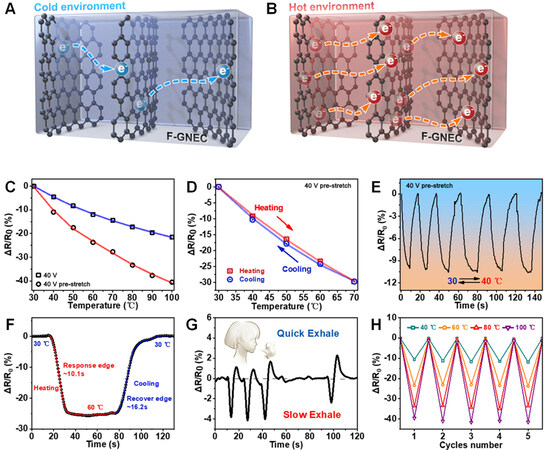
Figure 5. Temperature response of F-GNEC film. (A and B) Schematic diagram of temperature detection of F-GNEC film-based e-skin. (C) Comparison of ΔR/R0 versus external temperature between standard and pre-stretching film-based e-skin. (D) ΔR/R0 curves during heating and cooling process. (E) Multicycle of heating-cooling of the pre-stretching F-GNEC film. (F) Single temperature sensing response of pre-stretching F-GNEC film-based e-skin when heating to 60 °C and cooling to 30 °C. (G) Real-time response of detecting exhalation. (H) Stability and reliability test of pre-stretching F-GNEC film-based e-skin for five heating-cooling cycles under 40, 60, 80 and 100 °C.
The ΔR/R0 of the F-GNEC film-based e-skin at different temperatures was measured. As shown in Figure 5C, the ΔR/R0 values of the standard and pre-stretching F-GNEC film-based e-skin are represented by blue and red lines, respectively. For the standard F-GNEC film, when the temperature increases from 30 to 100 °C, the ΔR/R0 increases from 0 to -21.6%. Furthermore, the response of the pre-stretching F-GNEC film-based e-skin is -40.5% at 100 °C, which is about twice that of the standard F-GNEC film. Since its GN density is larger, the pre-stretching F-GNEC film-based e-skin has a stronger NTC phenomenon and its TC reaches -0.58%/°C, while the TC of the standard F-GNEC film only reaches -0.31%/°C. The 40 V F-GNEC film-based e-skin not only has a wide temperature measurement range but also has high sensitivity in the lower temperature range, indicating its potential for monitoring human body temperature.
Figure 5D shows the response of the pre-stretching F-GNEC film during the heating-cooling cycles. It can be seen that the pre-stretching F-GNEC film-based e-skin maintains a sensitive response during the heating and cooling process, indicating the stability and accuracy of its temperature detection performance. Subsequently, the response time of the temperature detection is measured. Figure 5E shows several heating-cooling cycles of the pre-stretching F-GNEC film-based e-skin from 30 to 40 °C. The resistance of the pre-stretching F-GNEC-based film can well follow the change in the ambient temperature. As shown in Figure 5F, the ΔR/R0 curve during a single heating and cooling process from 30 to 60 °C is shown. It can be seen that when the temperature is increased to 60 °C, the response time is ~10.1 s. When the temperature is maintained at 60 °C, the response of the e-skin remains stable. As the ambient temperature decreases to
Interestingly, the pre-stretching F-GNEC film was found to have the ability to detect the temperature of human breath, with the measurement result shown in Figure 5G. It can be seen that when the subject slowly exhaled, the ΔR/R0 of the pre-stretching F-GNEC film-based e-skin dropped to ~-4.1% and then slowly returned to 0%. When the subject quickly exhaled, the response then rose to 2.8%. Furthermore, the temperature detection stability of the pre-stretching F-GNEC film-based e-skin is measured. Figure 5H shows the ΔR/R0 value in heating-cooling cycles at 40, 60, 80 and 100 °C. It can be seen that after five heating and cooling cycles at different temperatures, the pre-stretching F-GNEC film-based e-skin maintains stable responses. These results reveal that the pre-stretching F-GNEC film-based e-skin has excellent temperature detection performance and the wide detection range allows the human body to perceive the external temperature. The outstanding sensitivity in the low-temperature range enables this e-skin to be used in medical testing and body temperature monitoring.
Decoupling of signals
The decoupling of the thermal and optical signals can be obtained by the response time. The optical response is much faster than the thermal response. The optical response is at the scale of 100-1000 ms, while the thermal response is in the range of 1-10 s. Hence, although there is a thermal drift of the carbon film while measuring the optical signal, the low-frequency electric signal can be easily filtered by the controlling circuit.
Application of F-GNEC film-based e-skin
In this study, the e-skin based on the pre-stretching F-GNEC film has not only the advantages of multi-response detection ability and fast response speed but also excellent stability. Subsequently, we integrate five F-GNEC film-based e-skin and fabricate the corresponding signal acquisition and processing circuits to finally obtain a multi-response data glove. Figure 6A presents the photographs when using the data glove for finger bending, temperature and photoelectric detection. It can be seen that the e-skin can fit the finger joints well, which benefits accurate measurements. The corresponding response is shown in Figure 6B. In mode 1, the user’s finger bends gradually while the data glove exhibits a stable response
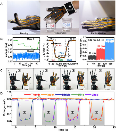
Figure 6. Comprehensive testing of F-GNEC film sensor gloves. (A) Photographs of bending, temperature and photodetection test while using F-GNEC-based e-skin data glove. (B) Response of F-GNEC-based e-skin in bending, temperature and photoelectric detection. (C) Photographs of four gestures when using F-GNEC-based e-skin data glove to control machine hand. (D) Corresponding real-time response of F-GNEC-based e-skin on different fingers when making the four gestures.
Subsequently, a Bluetooth module is added to the control circuit and the signals detected from the hand gestures are processed and transmitted to the machine hand. This allows the user to remotely control the machine hand through the data glove [Supplementary Video 1]. Figure 6C shows four postures of the machine hand using the F-GNEC film-based e-skin to control it. The corresponding response of each finger is shown in Figure 6D. It can be seen that the F-GNEC film data glove can well capture the movement of the hand and control the machine hand to make the corresponding posture. At present, the fields of VR technology and medical monitoring need a high-sensitivity and fast-response detector and F-GNEC-based e-skin could be a very promising candidate.
CONCLUSIONS
In summary, an ECR system was used to prepare a new F-GNEC film on a flexible PI substrate for the fabrication of multi-response e-skin. In addition, the higher substrate bias was used to increase the GN density. The GNs could be used as electron capture centers and form a conductive net. When external stress was applied, the spacing of the GNs increased and the conductivity of the conductive net changed. For tensile strain, the pre-stretching F-GNEC film-based e-skin exhibited not only a GF of 14,699 at ε = 0.5 % but also excellent stability. When measuring the bending angle, the ΔR/R0 value was as high as 113.2% at
DECLARATIONS
AcknowledgmentsThanks to Silver Basis Tech. Co. Ltd. for sealing the sensor using the IME technique. Thanks to Shenzhen MileBot Robotics Co., Ltd for providing the dexterous robot hand. The authors wish to acknowledge the assistance on TEM / FIB received from the Electron Microscope Center of Shenzhen University.
Authors’ contributionsConceived and designed the work: Zhang X, Li X, Wang X, Wen B
Supervised the overall project: Zhang X, Diao D
Methodology and fabrication: Li X, Wang X, Yuan L, Ye J
Characterization and testing: Li X, Deng H, Wang X
Manuscript writing and revision: Zhang X, Li X, Wang X, Diao D
Availability of data and materialsThe datasets generated and analyzed during the current study are available from the corresponding author upon reasonable request.
Financial support and sponsorshipThe authors gratefully acknowledge the financial support from the National Natural Science Foundation (Nos. 52275565 and 62104155) of China, NSF of Guangdong province (No. 2022A1515011667), and Guangdong Kangyi Special Fund (No. 2020KZDZX1173).
Conflicts of interestAll authors declared that there are no conflicts of interest.
Ethical approval and consent to participateNot applicable.
Consent for publicationNot applicable.
Copyright© The Author(s) 2022.
Supplementary MaterialsREFERENCES
1. Jing X, Wang X, Mi H, Turng L. Stretchable gelatin/silver nanowires composite hydrogels for detecting human motion. Mater Lett 2019;237:53-6.
2. Paul SJ, Elizabeth I, Gupta BK. Ultrasensitive wearable strain sensors based on a VACNT/PDMS thin film for a wide range of human motion monitoring. ACS Appl Mater Interfaces 2021;13:8871-9.
3. Yang Z, Wang DY, Pang Y, et al. Simultaneously detecting subtle and intensive human motions based on a silver nanoparticles bridged graphene strain sensor. ACS Appl Mater Interfaces 2018;10:3948-54.
4. Guan F, Guo CF. Flexible, high-strength, and porous nano-nano composites based on bacterial cellulose for wearable electronics: a review. Soft Sci 2022;2:16.
5. You A, Zhang X, Peng X, Dong K, Lu Y, Zhang Q. A Skin-inspired triboelectric nanogenerator with an interpenetrating structure for motion sensing and energy harvesting. Macro Mater Eng 2021;306:2100147.
6. Das PS, Chhetry A, Maharjan P, Rasel MS, Park JY. A laser ablated graphene-based flexible self-powered pressure sensor for human gestures and finger pulse monitoring. Nano Res 2019;12:1789-95.
7. Kireev D, Okogbue E, Jayanth RT, Ko TJ, Jung Y, Akinwande D. Multipurpose and reusable ultrathin electronic tattoos based on PtSe2 and PtTe2. ACS Nano 2021;15:2800-11.
8. Liu X, Liu D, Lee JH, et al. Spider-web-inspired stretchable graphene woven fabric for highly sensitive, transparent, wearable strain sensors. ACS Appl Mater Interfaces 2019;11:2282-94.
9. Yi S, Wang L, Chen Z, et al. High-throughput fabrication of soft magneto-origami machines. Nat Commun 2022;13:4177.
10. Maisto M, Pacchierotti C, Chinello F, Salvietti G, De Luca A, Prattichizzo D. Evaluation of wearable haptic systems for the fingers in augmented reality applications. IEEE Trans Haptics 2017;10:511-22.
11. Marasco A, Buonincontri P, van Niekerk M, Orlowski M, Okumus F. Exploring the role of next-generation virtual technologies in destination marketing. J Dest Mark Manag 2018;9:138-48.
12. Yin J, Hinchet R, Shea H, Majidi C. Wearable soft technologies for haptic sensing and feedback. Adv Funct Mater 2021;31:2007428.
13. Boutry CM, Negre M, Jorda M, et al. A hierarchically patterned, bioinspired e-skin able to detect the direction of applied pressure for robotics. Sci Robot 2018;3:eaau6914.
14. Chen H, Song Y, Cheng X, Zhang H. Self-powered electronic skin based on the triboelectric generator. Nano Energy 2019;56:252-68.
15. Guo H, Lan C, Zhou Z, Sun P, Wei D, Li C. Transparent, flexible, and stretchable WS2 based humidity sensors for electronic skin. Nanoscale 2017;9:6246-53.
16. Yang JC, Mun J, Kwon SY, Park S, Bao Z, Park S. Electronic skin: recent progress and future prospects for skin-attachable devices for health monitoring, robotics, and prosthetics. Adv Mater 2019;31:e1904765.
17. Su Q, Zhang H, Chen S. Flexible and tandem quantum-dot light-emitting diodes with individually addressable red/green/blue emission. NPJ Flex Electron 2021:5.
19. Kar E, Bose N, Dutta B, Mukherjee N, Mukherjee S. Ultraviolet- and microwave-protecting, Self-Cleaning e-skin for efficient energy harvesting and tactile mechanosensing. ACS Appl Mater Interfaces 2019;11:17501-12.
20. Dong K, Wu Z, Deng J, et al. A stretchable yarn embedded triboelectric nanogenerator as electronic skin for biomechanical energy harvesting and multifunctional pressure sensing. Adv Mater 2018;30:e1804944.
21. Patel S, Ershad F, Zhao M, et al. Wearable electronics for skin wound monitoring and healing. Soft Sci 2022;2:9.
22. Yuan J, Zhu R, Li G. Self-powered electronic skin with multisensory functions based on thermoelectric conversion. Adv Mater Technol 2022:5.
23. Zhang Y, Zhao Y, Zhai W, et al. Multifunctional interlocked e-skin based on elastic micropattern array facilely prepared by hot-air-gun. Chem Eng J 2021;407:127960.
24. Parangusan H, Ponnamma D, Al-Maadeed MAA. Stretchable electrospun PVDF-HFP/Co-ZnO nanofibers as piezoelectric nanogenerators. Sci Rep 2018;8:754.
25. Sun B, McCay RN, Goswami S, et al. Gas-permeable, multifunctional on-skin electronics based on laser-induced porous graphene and sugar-templated elastomer sponges. Adv Mater 2018;30:e1804327.
26. Choi D, Jang S, Kim JS, Kim H, Kim DH, Kwon J. A highly sensitive tactile sensor using a pyramid-plug structure for detecting pressure, shear force, and torsion. Adv Mater Technol 2019;4:1800284.
27. Ferreira A, Correia V, Mendes E, Lopes C, Vaz JFV, Lanceros-mendez S. Piezoresistive polymer-based materials for real-time assessment of the stump/socket interface pressure in lower limb amputees. IEEE Sensors J 2017;17:2182-90.
28. Qiu J, Guo X, Chu R, et al. Rapid-response, low detection limit, and high-sensitivity capacitive flexible tactile sensor based on three-dimensional porous dielectric layer for wearable electronic skin. ACS Appl Mater Interfaces 2019;11:40716-25.
29. Tran M, Tung T, Sachan A, Losic D, Castro M, Feller J. 3D sprayed polyurethane functionalized graphene/carbon nanotubes hybrid architectures to enhance the piezo-resistive response of quantum resistive pressure sensors. Carbon 2020;168:564-79.
30. Guo Y, Guo Z, Zhong M, Wan P, Zhang W, Zhang L. A flexible wearable pressure sensor with bioinspired microcrack and interlocking for full-range human-machine interfacing. Small 2018;14:e1803018.
31. Zhu L, Wang Y, Mei D, Ding W, Jiang C, Lu Y. Fully elastomeric fingerprint-shaped electronic skin based on tunable patterned graphene/silver nanocomposites. ACS Appl Mater Interfaces 2020;12:31725-37.
32. Pyo S, Kim W, Jung HI, Choi J, Kim J. Heterogeneous integration of carbon-nanotube-graphene for high-performance, flexible, and transparent photodetectors. Small 2017;13:1700918.
33. Ren M, Zhou Y, Wang Y, et al. Highly stretchable and durable strain sensor based on carbon nanotubes decorated thermoplastic polyurethane fibrous network with aligned wave-like structure. Chem Eng J 2019;360:762-77.
34. Wang Y, Mao H, Wang Y, Zhu P, Liu C, Deng Y. 3D geometrically structured PANI/CNT-decorated polydimethylsiloxane active pressure and temperature dual-parameter sensors for man–machine interaction applications. J Mater Chem A 2020;8:15167-76.
35. Peng X, Dong K, Ye C, et al. A breathable, biodegradable, antibacterial, and self-powered electronic skin based on all-nanofiber triboelectric nanogenerators. Sci Adv 2020;6:eaba9624.
36. Zhao L, Qiang F, Dai SW, et al. Construction of sandwich-like porous structure of graphene-coated foam composites for ultrasensitive and flexible pressure sensors. Nanoscale 2019;11:10229-38.
37. Zhao T, Li J, Zeng H, et al. Self-powered wearable sensing-textiles for real-time detecting environmental atmosphere and body motion based on surface-triboelectric coupling effect. Nanotechnology 2018;29:405504.
38. Qiao Y, Wang Y, Jian J, et al. Multifunctional and high-performance electronic skin based on silver nanowires bridging graphene. Carbon 2020;156:253-60.
39. Guo R, Wang X, Yu W, Tang J, Liu J. A highly conductive and stretchable wearable liquid metal electronic skin for long-term conformable health monitoring. Sci China Technol Sci 2018;61:1031-7.
40. Zhang X, Xiang D, Zhu W, et al. Flexible and high-performance piezoresistive strain sensors based on carbon nanoparticles@polyurethane sponges. Compos Sci Technol 2020;200:108437.
41. Zhao X, Meng F, Peng Y. Flexible and highly pressure-sensitive ternary composites-wrapped polydimethylsiloxane sponge based on synergy of multi-dimensional components. Compos Part B Eng 2022;229:109466.
42. Pan F, Chen S, Li Y, et al. 3D graphene films enable simultaneously high sensitivity and large stretchability for strain sensors. Adv Funct Mater 2018;28:1803221.
43. Huang L, Diao D, Cao Y. Electrochemical corrosion behaviors of N-doped graphene sheets embedded carbon films in acid. Appl Surface Sci 2021;544:148781.
44. Zhang W, Diao D, Sun K, Fan X, Wang P. Study on friction-electrification coupling in sliding-mode triboelectric nanogenerator. Nano Energy 2018;48:456-63.
45. Zhang X, Tian L, Diao D. High-response heterojunction phototransistor based on vertically grown graphene nanosheets film. Carbon 2021;172:720-8.
46. Chen W, Zhang X, Diao D. Low-energy electron excitation effect on formation of graphene nanocrystallites during carbon film growth process. Appl Phys Lett 2017;111:114105.
47. Tang ZH, Xue SS, Li YQ, Zhu ZC, Huang P, Fu SY. One-step synthesis of microdome patterns for microstructured pressure sensors with ultra-high sensing performance. ACS Appl Mater Interfaces 2021;13:48009-19.
48. Xia P, Liu P, Wu S, et al. Highly stretchable and sensitive flexible resistive strain sensor based on waterborne polyurethane polymer for wearable electronics. Compos Sci Technol 2022;221:109355.
49. Zhai W, Zhu J, Wang Z, et al. Stretchable, sensitive strain sensors with a wide workable range and low detection limit for wearable electronic skins. ACS Appl Mater Interfaces 2022;14:4562-70.
50. Zhang X, Lin Z, Peng D, Diao D. Bias-modulated high photoelectric response of graphene-nanocrystallite embedded carbon film coated on n-silicon. Nanomaterials 2019;9:327.
51. Lin Z, Wang Z, Zhang X, Diao D. Superhydrophobic, photo-sterilize, and reusable mask based on graphene nanosheet-embedded carbon (GNEC) film. Nano Res 2021;14:1110-5.
52. Devaraj S, Munichandraiah N. Effect of crystallographic structure of MnO2 on its electrochemical capacitance properties. J Phys Chem C 2008;112:4406-17.
53. Quhe R, Ma J, Zeng Z, et al. Tunable band gap in few-layer graphene by surface adsorption. Sci Rep 2013:3.
54. Yoo S, Kim C, Shin J, et al. Characterization of an amorphous carbon film covering a Mo grid during in situ heating TEM study. Mater Charact 2013;78:31-6.
55. Ferrari AC, Libassi A, Tanner BK, et al. Density, sp3 fraction, and cross-sectional structure of amorphous carbon films determined by x-ray reflectivity and electron energy-loss spectroscopy. Phys Rev B 2000;62:11089-103.
56. Shakerzadeh M, Teo E, Sorkin A, Bosman M, Tay B, Su H. Plasma density induced formation of nanocrystals in physical vapor deposited carbon films. Carbon 2011;49:1733-44.
57. Cao R, Wang H, Guo Z, et al. Black phosphorous/indium selenide photoconductive detector for visible and near-infrared light with high sensitivity. Adv Opt Mater 2019;7:1900020.
58. Dan L, Elias AL. Flexible and stretchable temperature sensors fabricated using solution-processable conductive polymer composites. Adv Healthc Mater 2020;9:e2000380.
59. Liu C, Han S, Xu H, Wu J, Liu C. Multifunctional highly sensitive multiscale stretchable strain sensor based on a graphene/glycerol-kcl synergistic conductive network. ACS Appl Mater Interfaces 2018;10:31716-24.
60. Zhao S, Lou D, Zhan P, et al. Heating-induced negative temperature coefficient effect in conductive graphene/polymer ternary nanocomposites with a segregated and double-percolated structure. J Mater Chem C 2017;5:8233-42.
Cite This Article
Export citation file: BibTeX | RIS
OAE Style
Zhang X, Li X, Wang X, Yuan L, Ye J, Wang X, Deng H, Wen B, Diao D. Direct fabrication of high-performance multi-response e-skin based on a graphene nanosheet film. Soft Sci 2022;2:18. http://dx.doi.org/10.20517/ss.2022.18
AMA Style
Zhang X, Li X, Wang X, Yuan L, Ye J, Wang X, Deng H, Wen B, Diao D. Direct fabrication of high-performance multi-response e-skin based on a graphene nanosheet film. Soft Science. 2022; 2(4): 18. http://dx.doi.org/10.20517/ss.2022.18
Chicago/Turabian Style
Zhang, Xi, Xiaolin Li, Xusheng Wang, Lin Yuan, Jing Ye, Xin Wang, Hualin Deng, Bo Wen, Dongfeng Diao. 2022. "Direct fabrication of high-performance multi-response e-skin based on a graphene nanosheet film" Soft Science. 2, no.4: 18. http://dx.doi.org/10.20517/ss.2022.18
ACS Style
Zhang, X.; Li X.; Wang X.; Yuan L.; Ye J.; Wang X.; Deng H.; Wen B.; Diao D. Direct fabrication of high-performance multi-response e-skin based on a graphene nanosheet film. Soft. Sci. 2022, 2, 18. http://dx.doi.org/10.20517/ss.2022.18
About This Article
Copyright

Data & Comments
Data


 Cite This Article 27 clicks

 Like This Article 33
likes
Like This Article 33
likes


Comments
Comments must be written in English. Spam, offensive content, impersonation, and private information will not be permitted. If any comment is reported and identified as inappropriate content by OAE staff, the comment will be removed without notice. If you have any queries or need any help, please contact us at support@oaepublish.com.